| Wafer System | Application | |
|---|---|---|
| Polar/ Single | Cleaning
| Etching
Solvent
|
| Wet Bench | Cleaning
| Solvent Tool
Etching
|
| Hybrid | Wafer Support
| Soak & Spray
Plating
|
| Si / SiC | Wafer Reclaim | |
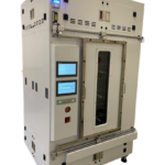
Polar/Single Wafer Wet Process
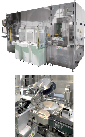
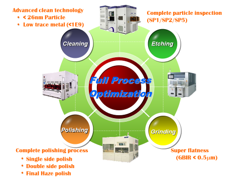
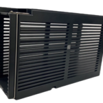
The Polar/Single series represents an advanced system for treating individual semiconductor wafers, widely used in FEOL processes to leverage the output quality. Compared to batch processing methods, single-wafer tools offer notable benefits such as superior process control, customization, decreased contamination risk, and enhanced yield. Single-wafer systems are versatile, can be applied to various applications, and are integrated with features like real-time monitoring, automated handling, and precise control, significantly improving reliability, efficiency, and productivity. These tools play a pivotal role in attaining high-quality semiconductor devices by enabling precise and controlled treatment on individual wafers.
| Cleaning | Etching | Stripper |
|---|---|---|
|
|
|
| Process | Application | Advantage |
|---|---|---|
|
|
|

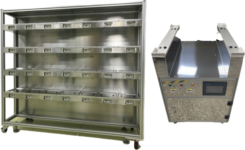
Wet Bench Process
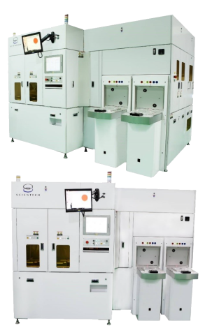
Wet bench systems process multiple wafers simultaneously and are widely used in BEOL processes, including cleaning, etching, and plating. Batch processing offers advantages in terms of throughput and efficiency, making it well-suited for high-volume applications. The equipment optimizes performance by using automated handling, precise chemical delivery, and control systems. Safety measures and waste treatment are integrated to ensure responsible chemical handling. Batch wet processing plays a crucial role in semiconductor manufacturing, enabling efficient and controlled treatment, and resulting in high-quality devices.
| Cleaning | Etching | Stripper |
|---|---|---|
|
|
|
| Process | Application | Advantage |
|---|---|---|
|
|
|
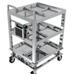
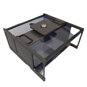
PR Stripper- Soak and Spray Module
PR Stripper (soak and spray module) is a hybridized tool designed to generate a high-quality output as a single wafer process while maintaining a high yield quantity as a bench process. It provides the ability to monitor and control the process of a specific individual wafer or a desired set of wafers. Furthermore, it allows for the concurrent usage of wafers of various sizes, such as 8-inch and 12-inch wafers, effectively eliminating solid and liquid film-resist products as well as metal lift-off in a cost-effective and efficient manner.
| Process | Application | Advantage |
|---|---|---|
|
|
|
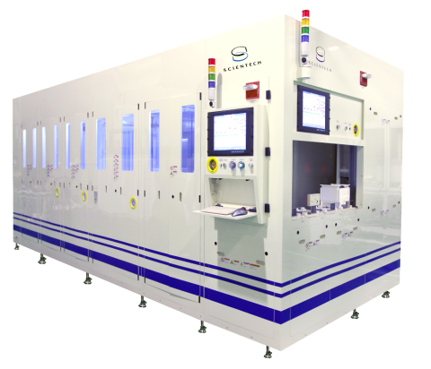
Temporary Bonding and Debonding
Temporary bonding and debonding are essential processes in semiconductor manufacturing. This technology involves temporarily bonding a device wafer to a carrier wafer using an intermediate material, which provides physical stability for thin wafers or wafers to be trimmed during processing. This allows the delicate device wafer to be processed with additional mechanical support. The wafer and carrier are debonded once the necessary processing steps are completed. In this tool, the wafer and carrier are bonded with adhesive through UV curing and debonded via IR laser at room temperature. These processes enable efficient handling and processing of wafers in semiconductor manufacturing.
| Process | Application | Advantage |
|---|---|---|
|
|
|
Temporary Bonding and Debonding- Aquila
Temporary bonding and debonding, Carriers are temporarily bonded to the wafer via thermal energy in the Aquila system, providing physical stability and high thermal resistance for subsequent back-end processes. UV laser emission is used to debond the wafer and carrier. Aquila system provides higher chemical and thermal resistance which enables the wafer to be utilized in advanced semiconductor processes such as metallization, TSV, bumping, UBM, RDL etc.
| Process | Application | Advantage |
|---|---|---|
|
|
|

Wafer Reclaim
12″ Wafer Reclaim
- Capacity: 160K / Month
- Cu and Non-Cu Process
SiC Wafer Reclaim Service
- SiC Wafer Reclaim Service: Grinding, Polishing and Reclaim Service
- Capacity: 1K / Month
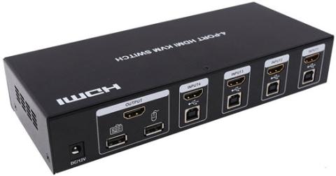
Remote Control System
Remote Control System (RCM) and KVM for in-line production monitor / control in semiconductor and flat panel display…industries.
Customized ESD Solution
- Metal Cassette / Metal Frame cassette by Customized Service
- Magazine by Customized Service
Cleanroom Support Solution
- Multifunctional Cleaning Equipment
- N2 Purge System
- Power Assist Cart